
When you think about semiconductor innovation, advanced nodes, novel materials, or sophisticated system architectures are what typically come to mind. Packaging is often viewed as a final step – a mere protective shell around the “real” technology, but for today’s devices, the package is key to device performance, reliability and connectivity. And the foundation of a successful IC package begins with the lead frame.
Why Lead Frames Matter in IC Packaging
While rarely viewed by most people, the humble lead frame enables the electrical, mechanical, and thermal performance that modern electronics demand. As devices become smaller, more powerful, and more densely integrated, the importance of getting the lead frame right has only increased.
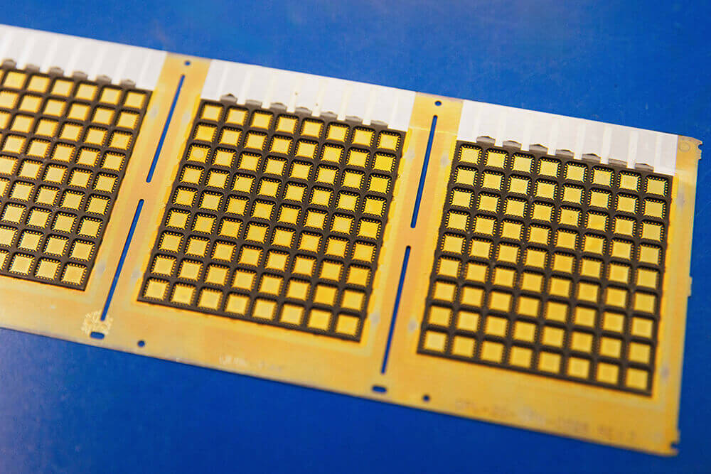
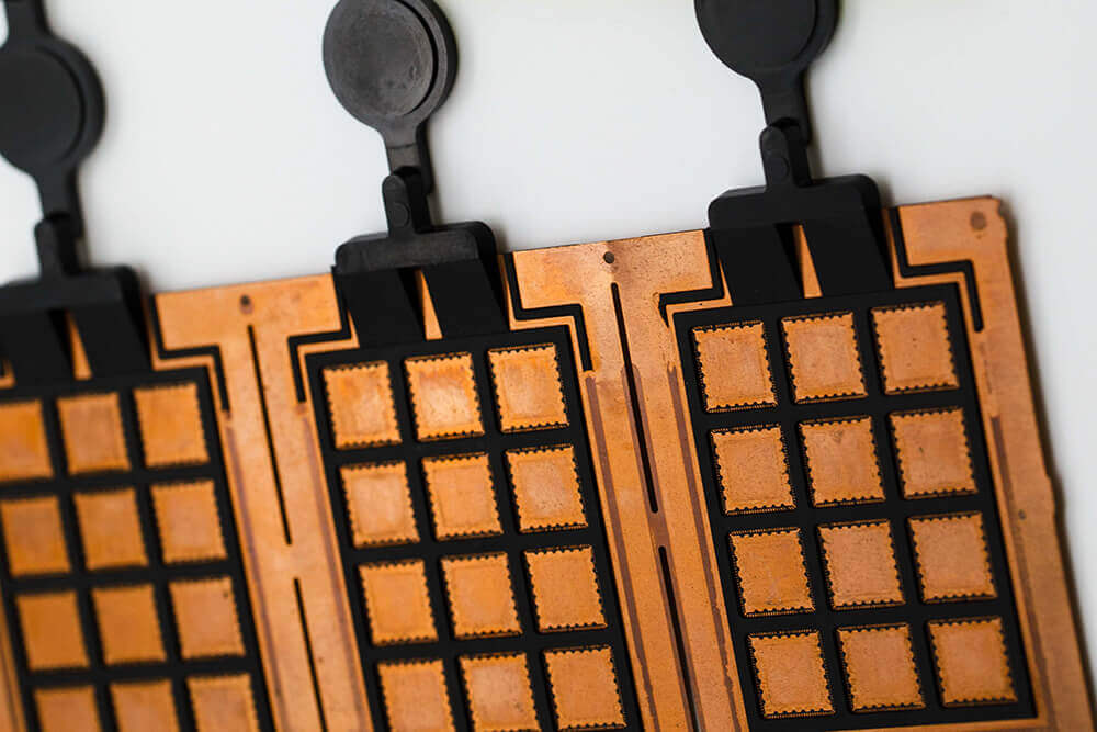
A lead frame is essentially a precision-stamped or etched metal structure that forms the internal skeleton of an IC package. It holds the die in place, provides electrical pathways from the die to the outside world, and serves as a primary path for heat to escape. Because it sits at the intersection of these functions, lead frame design directly influences device yield, long-term reliability, and real-world performance. A poorly optimized lead frame can introduce electrical parasitics, create thermal bottlenecks, or complicate assembly, but a well-designed one helps ensure consistent wire bonding, stable die attach, and efficient heat dissipation over the product’s lifetime.
QP Technologies’ Approach to Semiconductor Assembly
This is where thoughtful design and close coordination with assembly processes matter. Rather than treating lead frames as generic commodities, some packaging providers invest in designing them with the end application in mind. QP Technologies takes this approach, developing select lead frames in-house to better align package design with die requirements and assembly flows – giving customers greater control, faster development cycles, and consistent design quality.
In practical terms, in-house design enables tighter collaboration between design and manufacturing teams. Die geometry, bond pad layout, and wire bonding strategies can be considered alongside lead frame geometry from the start, rather than forced to fit a pre-existing template. This can be especially valuable for custom devices, niche applications, and low- to mid-volume programs where flexibility and responsiveness are critical. Material selection and plating choices are another area where early design involvement pays off. Different finishes can affect wire bondability, corrosion resistance, and overall reliability.
Controlling these variables through working with QP Technologies, while maintaining design ownership, helps the customer preserve design intent from concept through finished device, leveraging trusted external fabrication resources for production.
Our Broad Lead Frame Offerings
Lead frames remain highly relevant across a range of established and emerging package types. Quad flat no-lead (QFN) and dual flat no-lead (DFN) packages, for example, are widely used because they offer compact footprints and strong thermal performance for surface-mount applications. Even legacy formats like small-outline IC (SOIC) continue to serve industrial and long-lifecycle markets where proven reliability and supply stability are paramount. In all of these cases, the lead frame plays a central role in how the package ultimately performs in the field.
| QFN Package Sizes | DFN Package Sizes | SOIC Package Sizes |
| 3×3 mm – 8, 12, 16 leads | 1.5×1.5 mm – 6 leads | 8 leads |
| 4×4 mm – 16, 20, 24, 28, 32 leads | 2×2 mm – 6 & 8 leads | 14 leads |
| 5×5 mm – 20, 24, 28, 32, 36, 40 leads | 3×3 mm – 8 & 10 leads | |
| 6×6 mm – 40, 48, 52 leads | 3×2 mm – 10 & 12 leads | |
| 7×7 mm – 48, 56, 60 leads | 4×3 mm – 12 leads | |
| 8×8 mm – 52, 56, 68 leads | 4×4 mm – 12 leads | |
| 9×9 mm – 64 leads | ||
| 10×10 mm – 72 leads | ||
| 11×12 mm – 76 leads | ||
| 12×12 mm – 80, 88, 100 leads |
Our in-house lead frame design integrates seamlessly with QP Technologies’ complete IC assembly services, including:
- Die prep
- Die attach
- Wire bonding
- Overmolding/encapsulation
- Marking and singulation
- Environmental, mechanical, and electrical testing
Lead Frames Built for Today, Ready for Tomorrow
Lead frames’ success depends on how well they integrate with the full assembly flow — from die attach and wire bonding to molding, marking, and singulation. A packaging strategy that considers these steps holistically can reduce development friction and lower overall risk. For customers, that often translates into smoother transfers from design to production and fewer surprises during qualification.
As the industry pushes toward higher performance and smaller form factors, it is tempting to focus only on the most visible innovations. Lead frames may be hidden inside the package, but they remain a quiet enabler of the electronics that power everyday life — from industrial systems to consumer devices — and a reminder that in semiconductor packaging, details matter.
Contact QP Technologies today to select the lead frame assembly solution that meets your product development needs.