The push to create smaller, thinner and denser chip packages is on… and has been for some time. A few years ago, it became clear that the way forward for the semiconductor industry was to intensify the focus on heterogeneous integration (HI)—integrating separately manufactured components into a system-in-package (SIP), a higher-level assembly. Such packages afford power-efficient, high-bandwidth connections between components within a compact form factor, providing enhanced functionality and improved operating characteristics.
To optimize these packages for use in consumer, communications and other high-demand end products that need to be smaller and faster with lower power consumption, they have to be as thin as possible. To go thin, we have to grind and spin. Backgrinding is a key step in wafer preparation, and providers like Quik-Pak are grinding wafers increasingly thinner all the time.
Quik-Pak can perform automated, volume backgrinding of a cassette containing up to 25 whole wafers, from 100mm to 200mm (4 to 8 inches) in diameter, as well as partial wafers, 300mm (12-inch) quartered wafers and even individual die. We can thin 300mm wafers down to 75 microns, and 200mm and smaller wafers down to 25 microns. We can also thin and polish such materials as gallium nitride (GaN), glass, quartz and ceramic.
Other packages that Quik-Pak can address through its wafer-prep capabilities include ball grid arrays (BGAs) with flip-chip and ball attach. Flip-chip can be thinned to 4 mils, or 100 microns. We can also thin bumped wafers, which requires special tape that doesn’t damage bumps when thinning them down to down to less than 100 microns.
As wafers continue to be ground ever thinner—in some cases, people are looking to grind down to as low as 5 microns—physical limitations loom, which will create new challenges. Regardless, thinning wafers pose integrity issues that must be addressed and mitigated.
The DAF distinction
Commercially available since 2000, die-attach film (DAF) has become essential in the HI era for use in wafer prep and singulation of wire-bonded single and multi-chip stacked solutions. Applied to the backside of the wafer, highly adhesive DAF serves as the adherent material for the die and as the support film. Once wafer singulation is complete, the DAF-protected die are picked off the support tape and placed on the substrate. Multiple die are then stacked vertically in a slanted/offset pattern, and the die are wire-bonded on the edges.
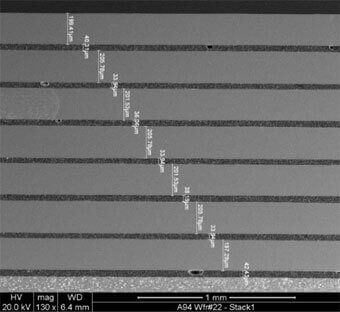
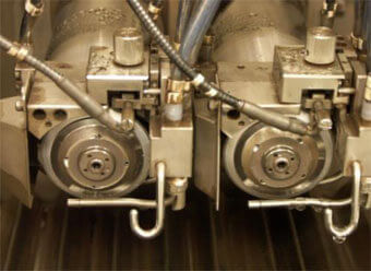
The example in Figure 1 shows a cross section of a stacked-die device with seven die layers created using a diamond-filled DAF. The silicon wafers were thinned to 200 microns before laminating onto the DAF, and the die on the DAF-treated device wafers were singulated using a dual-spindle dicing saw, as shown in Figure 2.
Whereas paste can outgas, void and bleed into other areas, DAF is easily controlled. It allows not only the sharp edges and shape of the die to be maintained, but also the die footprint since the die and film are cut simultaneously. DAFs can also be applied to non-die-attach processes such as lid sealing and wafer bonding.
Quik-Pak’s expertise in DAF is a key aspect of our wafer prep capabilities and a competitive differentiator. Working with our suppliers, who provide DAF in sheets for non-automated lamination, we can offer a variety of conductive and non-conductive DAF for customers to choose from. Ensuring that the films are always in stock requires a high degree of commitment, as the films last about 6 to 12 months when stored at temperatures between 0-10°C. Beyond this timeframe, their physical properties change, and the films begin to deteriorate; they can be stored at room temperature, but this cuts their shelf life in half.
As keeping the films in stock can be challenging, few stateside suppliers make them available. Moreover, while the cost per wafer using DAF may be higher, the savings in process steps and yield improvement make the overall cost comparable to using paste for wafer prep, creating a significant benefit for our customers. Another advantage is that, since most customers eventually go offshore to have the HI prototypes we create for them manufactured in high volumes, supporting DAF is vital, as it is being used overseas for this purpose.
HI Roadmap Evolving
As a result of the industry’s pivot toward HI, the industry blueprint for advancement has transitioned from the longtime ITRS [International Technology Roadmap for Semiconductors], which ended in 2016, to the Heterogeneous Integration Roadmap (HIR). The HIR provides a long-term vision for the electronics industry, identifying difficult future challenges and potential solutions. Its sponsors represent a broad cross-section of the global electronics community: IEEE Electronics Packaging Society, IEEE Electron Devices Society, IEEE Photonics Society, SEMI, and the Electronic and Photonic Packaging Division of the American Society of Mechanical Engineers. The 2019 HIR edition was released in October 2019.
The upcoming third annual HIR Meeting and Symposium, to be held next week in Silicon Valley, will kick off revision efforts for the 2020 edition. Quik-Pak parent Promex Industries is a sponsor and worked with ASE Group to organize the event. More than 150 attendees from industry-leading global companies are expected.
The Symposium is open to the general public, and will be held Thursday, Feb. 20, from 8:30 AM – 6:00 PM. The Technical Working Meeting and Open House will be held Friday, Feb. 21, from 8:30 AM – 4:00 PM Get further details and register. If you’re unable to attend, we’ll provide a summary of the symposium here after the event.
It’s an exciting time for the industry—I hope to see you there!