As noted in last month’s blog post, the semiconductor industry has turned its efforts toward the ongoing fleshing out of a roadmap focused on advancing heterogeneous integration (HI). HI integrates separately manufactured components into higher-level assemblies such as systems-in-package (SiPs), offering higher bandwidth and functionality and lower power consumption in a small form factor. This approach is acknowledged by the industry as the way to ensure industry innovation continues to move forward.
The Heterogeneous Integration Roadmap (HIR) – sponsored by industry organizations and their members from across the global electronics ecosystem – was developed to lay out a long-term vision for the electronics industry, and includes challenges to be overcome, as well as potential solutions. The 2019 HIR edition was released last October, and industry contributors are now actively working on the 3rd edition. It should be noted that these efforts may be impacted by interruptions or slowdowns in production necessitated by worldwide efforts to rein in the spread of the novel coronavirus (COVID-19). The Technical Working Group (TWG) that I co-chair, along with Bill Chen of ASE, is focused on single-chip and multi-chip packaging for HI.
Connectivity drives all
As SEMI President Ajit Manocha noted in his opening comments at the third annual HIR Symposium in February, new disruptions are driving exponential growth in the IC industry, which is expected to be worth $500 billion within five years and $1 trillion in the next 10-15 years. Drivers to the trillion mark will include 6G, quantum computing, smart manufacturing, blockchain technology, neuromorphic computing, the growing digital economy – all of which is underpinned by the prime driver: connectivity.
It’s estimated that there will be a trillion connected devices on the planet by 2030. To put this in perspective, currently, there are approximately 30 billion, with more than 200 million being added every day. This brings into sharp focus the need for HI-optimized solutions across the entire tech spectrum, from design to materials, to production, packaging and test, to end products and various industry applications.
The HIR Symposium included presentations from all of the Technical Working Groups, of which there are currently more than two dozen. Some key trends that emerged from the fast-paced presentations include:
- Growing use of chiplets – chiplets are not a new concept, but as part of the “More than Moore” movement they’ve become a hot commodity. Chiplets offer advantages for scaling and yield in a range of applications, such as building critical systems and subsystems for aerospace and defense. Our TWG is collaborating with high-performance computing (HPC), 3D, test and other areas to develop guidelines for HI utilizing chiplets in single- and multi-chip packaging.
- Continued rise of flexible electronics – Flexible electronics are a highly attractive option for wearable sensors used in healthcare and extreme-performance applications. New applications being considered include flexible/stretchable power sources and advanced, flexible lithium-ion batteries that can help take Li-ion technology beyond its existing limitations. A prime example of heterogeneous integration, flex electronics must integrate devices, power and data management, and packaging considerations to be addressed include heat sink and biocompatibility.
- Big Data applications. In high-performance computing and data collection, emerging HI applications demand domain-specific accelerators, which integrate analytics, Big Data processing and the internet of things (IoT). Pradeep Dubey of Intel, in his plenary address, described how we are moving from a world to analytical models to one of data-driven models. As a results, artificial intelligence (AI) compute needs are massive even for simple applications, creating challenges for HI integration and packaging.
The industry workhorse: chip integration
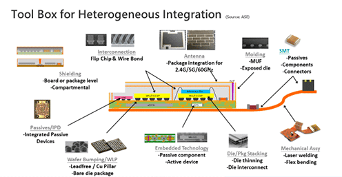
When Dave Chen summarized during the HIR Symposium the work done by our TWG, he referred to single- and multi-chip integration as “the workhorse of the industry.” Our category comprises a wide range of package types and related technologies, as the below figure—developed by ASE and borrowed from our chapter in the HI Roadmap—illustrates.

The purpose of HI is to build large systems out of smaller functions, i.e., systems-in-package (SiPs), which are separately designed, packaged, interconnected and manufactured. The chapter our TWG developed in the roadmap lays out the basic tool sets—infrastructure & knowledge—for HI for all the market segments.
Currently, in addition to looking at chiplets, we are investigating some key areas and challenges to be addressed in the next version of the roadmap. These include:
- Substrates for very large packages
- Reliability issues for advanced packaging
- Chip package interaction at lower-digit nodes
- Materials for additive manufacturing (i.e., 3D printing)
- Board-level power integration
- Adding to the classical electromigration model
These are just some of the issues for which we are looking to provide some insight and potential answers in the next rev of the Heterogeneous Integration Roadmap. And, as all the TWG chairs noted during the symposium, we welcome the addition of and input from new members. If you would like to contribute to our efforts or would like to know more about our working group, please feel free to contact me at annetteteng@promex-ind.com.
